

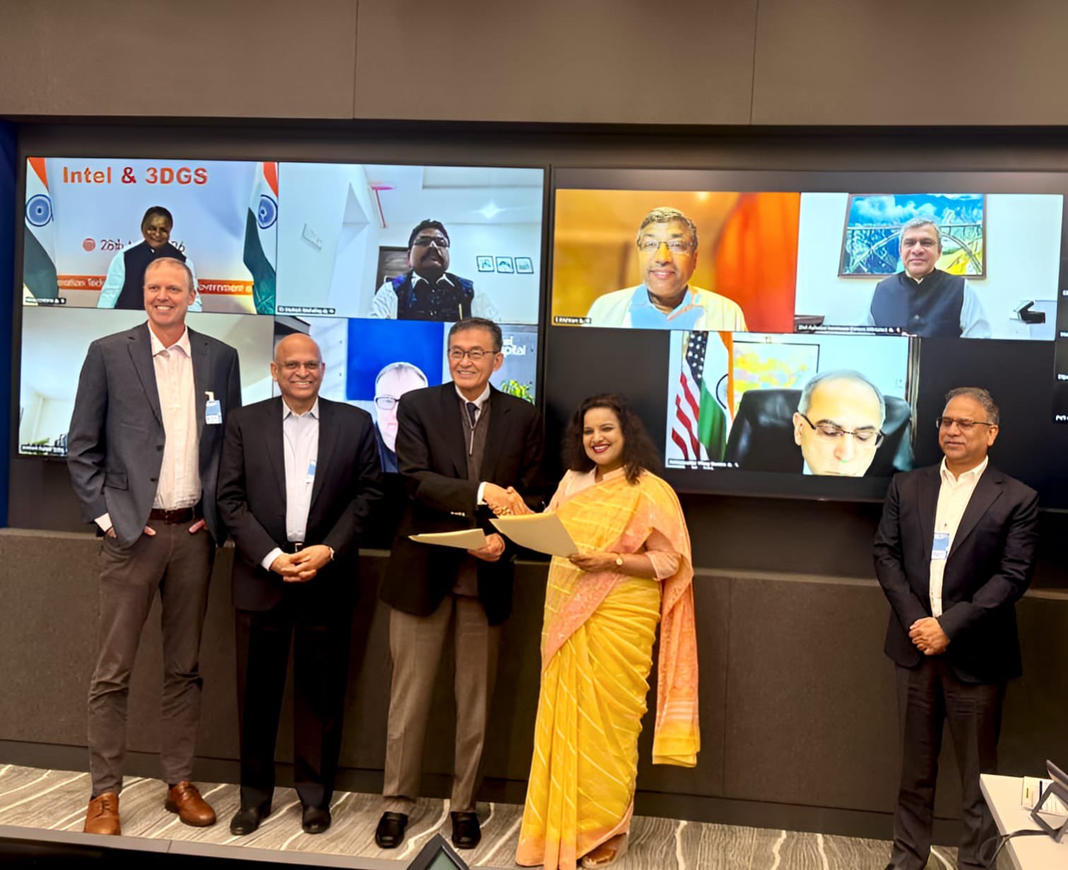

Intel, Odisha Government and 3DGS Sign Landmark MoU for Advanced Packaging Facility
In a major boost to India’s semiconductor and high-technology manufacturing ambitions, the Government of Odisha, Intel Corporation, and 3DGS Inc. USA have signed a landmark Memorandum of Understanding to establish an Advanced Packaging Glass Core Substrate Manufacturing Facility in Odisha.The MoU was signed in the presence of Union Minister for Electronics and IT Ashwini Vaishnaw, Odisha Chief Minister Mohan Charan Majhi, Intel CEO Lip-Bu Tan, and several senior dignitaries.The proposed facility, to be developed in the Bhubaneswar–Khurda region, is expected to attract an estimated investment of around USD 3.3 billion, making it one of the largest high-technology manufacturing investments in India.Speaking on the occasion, Union Minister Ashwini Vaishnaw said the agreement aligns with the Government of India’s vision to build a complete semiconductor manufacturing ecosystem in the country. He highlighted that the entry of global technology giants such as Applied Materials, Lam Research, Tokyo Electron, and Merck Electronics reflects growing international confidence in India’s semiconductor sector.He also mentioned the recent collaboration between Tata Electronics and Dutch multinational ASML as another milestone for India’s expanding semiconductor ecosystem.The upcoming facility will focus on advanced packaging glass core substrates, high-density interconnect substrates, and associated semiconductor technologies. Intel will provide technology know-how and process expertise for the project.Officials stated that the project will be implemented in multiple phases over the next five to six years. Once operational, the facility is expected to create more than 1,800 direct high-skilled employment opportunities while also generating significant indirect jobs across manufacturing, logistics, and technology sectors.The initiative is part of the larger India Semiconductor Mission aimed at strengthening domestic manufacturing, boosting supply chain capabilities, and positioning India as a global semiconductor hub.The project is also expected to transform Odisha into a major destination for semiconductor manufacturing and digital infrastructure development, further enhancing the state’s role in India’s high-tech industrial growth story.